What is outsourced hardware development?
Outsourced hardware development means engaging an external engineering partner to design, prototype, test, and industrialize electronic hardware on your behalf. Done well, it reduces time-to-market by 30–50% compared to building an in-house team from scratch, while providing immediate access to specialized capabilities (FPGA design, RF engineering, EMC compliance) that most companies don't maintain internally.
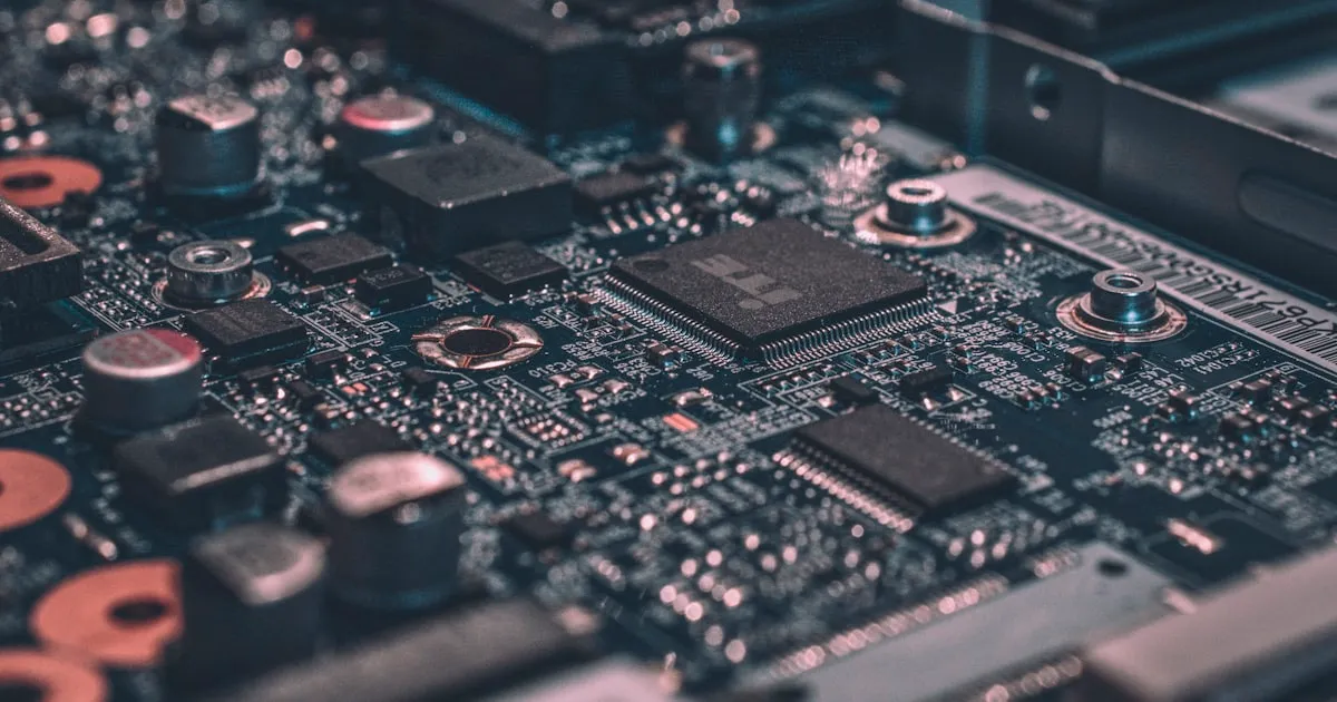
However, outsourcing hardware is fundamentally different from outsourcing software. A bug in firmware can be patched remotely; a bug in a PCB layout requires a respin costing €5,000–50,000 and 4–8 weeks of delay. This article provides a technical decision framework for making outsourced hardware development successful.
Choosing the Right Partner: Evaluation Criteria
Not all hardware development partners are equal. Here’s what to evaluate:
| Criterion | What to Look For | Red Flags |
|---|---|---|
| Technical depth | Named engineers with specific domain expertise (FPGA, RF, power, EMC) | “We do everything” with no specialization details |
| Reference designs | Published case studies with quantified outcomes | Only stock photos, no real project evidence |
| Toolchain maturity | Altium Designer, Vivado, Quartus, KiCad — industry-standard EDA tools | Outdated or unspecified tools |
| Testing capability | In-house pre-compliance EMC, environmental testing, functional test development | ”Testing handled by third party” with no details |
| Certification experience | Track record of CE, FCC, MIL-STD, medical device approvals | No mention of regulatory experience |
| Supply chain | Dual-source strategy, buffer stock, REACH/RoHS compliance documentation | Single-source components, no BOM risk analysis |
| IP ownership | Client owns 100% of all deliverables (schematics, Gerbers, firmware, RTL) | Shared IP or license-back clauses |
Engagement Models
| Model | NRE Structure | Best For | Risk Profile |
|---|---|---|---|
| Fixed-price | Defined scope, fixed cost | Well-defined projects with clear requirements | Low risk for client, higher NRE premium |
| Time & Materials | Hourly/daily rates | Exploratory, R&D-heavy projects | Client carries scope risk |
| Hybrid | Fixed milestones + T&M for exploration | Most real-world projects | Balanced risk sharing |
| Retained team | Dedicated engineers on monthly retainer | Ongoing product evolution | Lowest per-hour cost, requires pipeline |
The V-Model: How Professional Hardware Development Works
Professional outsourced hardware follows the V-model methodology, where each design phase has a corresponding verification phase:
Requirements Definition ←→ System Acceptance Testing
  System Design ←→ System Integration Testing
    Hardware Design ←→ Hardware Verification (EMC, environmental)
      Detailed Design (schematic, PCB) ←→ Unit Testing (component level)
        Manufacturing ←→ Production Testing (EOL, ICT)
Critical Milestone Gates
Every project should have clearly defined gates with deliverables:
- Concept Review (CR) — Requirements specification, feasibility analysis, technology selection, preliminary BOM costing
- Design Review (DR) — Schematic complete, BOM finalized, simulation results (SPICE, signal integrity), PCB stackup defined
- Prototype Review (PR) — First prototype assembled and tested, initial EMC pre-compliance results, firmware baseline functional
- Design Validation (DV) — Full functional testing, environmental testing (thermal, vibration), EMC compliance, regulatory pre-assessment
- Production Validation (PV) — Production line qualified (PPAP), end-of-line test fixtures designed, first article inspection approved
NRE Planning: What Hardware Development Actually Costs
A complete hardware development program typically breaks down as follows:
| Phase | % of NRE | Typical Duration | Key Deliverables |
|---|---|---|---|
| Requirements & feasibility | 5–10% | 2–4 weeks | Requirements spec, technology trade study |
| Schematic & PCB design | 25–35% | 4–8 weeks | Schematic, BOM, PCB layout, Gerber files |
| Prototyping | 15–20% | 3–6 weeks | Assembled prototypes (5–20 units) |
| Firmware development | 15–25% | 4–12 weeks | Production firmware, bootloader, OTA |
| Testing & certification | 15–25% | 4–8 weeks | EMC, safety, environmental test reports |
| Production tooling | 5–10% | 2–4 weeks | Test fixtures, programming jigs, process docs |
Total NRE for a moderately complex IoT product (4-layer PCB, wireless connectivity, sensor array, enclosure): typically €40,000–120,000 depending on complexity, certification requirements, and regulatory scope.
Risk Mitigation Strategies
Hardware development risks are fundamentally different from software risks:
- Component availability — Verify stock and lead times before committing to a BOM. Maintain dual-source alternatives for every critical component. The 2020–2023 chip shortage taught the industry that single-source dependency is an existential risk
- Signal integrity — Simulation before fabrication. High-speed signals (>100 MHz), DDR memory interfaces, and RF traces require pre-layout simulation using tools like HyperLynx or Ansys HFSS
- EMC compliance — Pre-compliance testing after the first prototype, not at the end. A failed EMC test at the certification lab costs €3,000–5,000 per test iteration plus 2–4 weeks of redesign
- Thermal management — CFD simulation and thermal imaging of prototypes. A design that works at 25°C may fail at 55°C industrial ambient
Why Inovasense?
We operate as a One Stop Shop — the same engineering team handles requirements, design, prototyping, testing, certification, and production support. This eliminates the coordination overhead, communication gaps, and intellectual property fragmentation that occur when multiple vendors handle different phases.
All development is performed within the EU, with full IP ownership transferred to the client. We sign mutual NDAs before any technical discussion, and all deliverables (schematics, Gerbers, RTL, firmware source) are the client’s property. Contact us to discuss your project.
Sources & Official References
- RoHS Directive — 2011/65/EU — EUR-Lex (Official Journal of the EU)
- REACH — Regulation (EC) No 1907/2006 — EUR-Lex (Official Journal of the EU)
Related guides inIndustrial Design & Process
Explore all →V-Model in Electronics Development
A structured V-model approach in electronics development prevents costly PCB respins, EMC failures, and certification delays. Learn the methodology.
Outsourced Hardware Development ROI: 2026 Cost Breakdown
Outsourced hardware development cuts time-to-market by 30–50% and saves €500K–2M in CapEx. 2026 ROI breakdown with real cost comparison.