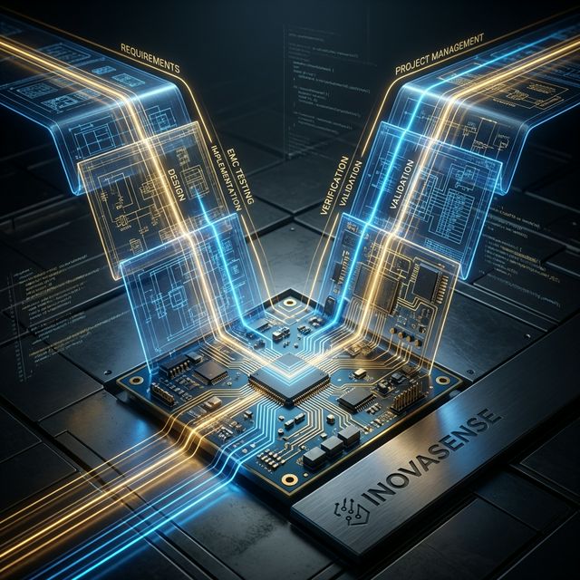
The V-model is the established systems engineering methodology for hardware development, where every design phase on the left side of the “V” has a corresponding verification phase on the right side. Unlike agile software development (where iterating is cheap), hardware iteration is expensive — a PCB respin costs €5,000–50,000 and delays a project by 4–8 weeks. A comprehensive, structured approach isn’t bureaucratic overhead; it’s the only way to predictably deliver hardware on time and on budget.
Why Hardware Projects Fail
Before examining the methodology, it’s worth understanding what goes wrong in projects that don’t follow one:
| Failure Mode | Root Cause | Cost of Late Discovery |
|---|---|---|
| EMC non-compliance | No pre-compliance testing before certification lab | €3,000–5,000 per failed test + 4–8 week respin |
| Thermal shutdown | No thermal simulation, works at 25°C but fails at 55°C | PCB redesign, new heatsink/enclosure tooling |
| Power supply instability | Inadequate decoupling, missing SPICE simulation | Board respin, potential component damage in field |
| Component obsolescence | No lifecycle check on BOM components | Redesign around replacement part, new PCB revision |
| Regulatory gap | Certification requirements not considered in architecture | Fundamental architecture change, project restart |
Every one of these failures is preventable with proper upfront planning and structured verification.
The V-Model in Practice
Left Side: Design Decomposition
1. Requirements Definition (2–4 weeks)
- Functional requirements (what the product must do)
- Non-functional requirements (temperature range, EMC class, IP rating, certifications needed)
- Interface specifications (connectors, communication protocols, mechanical constraints)
- Regulatory requirements mapping (CE, FCC, MIL-STD, medical class, ATEX zone)
2. System Architecture (1–2 weeks)
- Block diagram with defined interfaces between subsystems
- Technology selection trade study (MCU vs SoC vs FPGA, wireless protocol, sensor selection)
- Power budget analysis (total current draw, battery sizing, thermal dissipation estimate)
- Preliminary BOM with component availability and lead time verification
3. Detailed Design (4–8 weeks)
- Schematic capture in Altium Designer or KiCad
- PCB layout with impedance-controlled stackup for high-speed signals
- SPICE simulation of power supply, analog circuits, and critical signal paths
- Signal integrity simulation for DDR, high-speed serial, and RF traces (HyperLynx, Ansys HFSS)
- Mechanical integration (3D model, thermal simulation, DFM review)
Bottom of the V: Build
4. Prototype Fabrication (3–6 weeks)
- PCB fabrication (typically 4–6 layer, FR-4 or Rogers for RF)
- Component procurement and incoming inspection
- SMT assembly (pick-and-place, reflow, through-hole)
- Initial bring-up and power-on testing
Right Side: Verification (Maps to Design Phases)
5. Unit Testing (verifies Detailed Design)
- Individual subsystem verification (power supply output voltage, ripple, efficiency)
- Peripheral communication (SPI, I²C, UART, CAN waveform analysis with logic analyzer)
- Analog circuit performance (gain, bandwidth, noise floor)
6. Integration Testing (verifies System Architecture)
- Complete system functional testing
- Firmware integration and system-level debugging
- Communication protocol validation (wireless range testing, packet error rate)
- Power consumption profiling (Nordic PPK2 or Otii Arc for µA-level measurement)
7. System Verification (verifies Requirements)
- EMC pre-compliance (conducted/radiated emissions, susceptibility)
- Environmental testing (thermal cycling -40°C to +85°C, vibration per IEC 60068, humidity)
- Safety testing (dielectric withstand, leakage current, ground continuity per EN 62368-1)
- Regulatory certification submission (CE marking, FCC Part 15, specific industry certifications)
8. Acceptance Testing (verifies Requirements Definition)
- Customer acceptance criteria validation
- Field trial / pilot deployment
- Production readiness review
Communication: The Hidden Success Factor
In outsourced development, communication quality directly determines project outcomes:
- Weekly status reports — Progress against milestone plan, open risks, decisions needed
- Design review meetings — Formal reviews at each gate (CR, DR, PR, DV, PV) with documented minutes and action items
- Issue tracking — Every bug, design question, and change request tracked with priority and owner
- Change control — Any requirement change after Design Review requires formal change request with impact assessment (cost, schedule, certification)
The most expensive words in hardware development are “while we’re at it, can we also…?” without a corresponding change control process.
Quality Metrics We Track
| Metric | Target | Why It Matters |
|---|---|---|
| First-pass yield | >95% | Measures manufacturing quality and design robustness |
| EMC pre-compliance pass rate | >80% first attempt | Early testing catches issues before expensive lab visits |
| Requirement traceability | 100% coverage | Every requirement has a corresponding test |
| BOM dual-source coverage | >90% of line items | Supply chain resilience |
| Design review action closure | 100% before next gate | Unresolved actions compound into late-stage failures |
At Inovasense, the V-model isn’t a document — it’s how every project is structured. Each milestone gate has defined entry/exit criteria, and we don’t proceed until the previous gate’s deliverables are complete and reviewed. This disciplined approach is why our projects deliver on time and pass certification on the first submission. Contact us to start with a proper requirements review.