What is an FPGA?
An FPGA (Field-Programmable Gate Array) is a semiconductor device containing thousands to millions of configurable logic blocks that can be programmed — and reprogrammed — to implement any digital circuit. Unlike a CPU that executes software instructions sequentially, an FPGA physically rewires itself to become the hardware you design, enabling massively parallel processing with deterministic, nanosecond-level latency. FPGAs are used in 5G infrastructure, defense radar, medical imaging, autonomous vehicles, and Edge AI systems. For custom FPGA-based product development, see our FPGA Design Services.
Why FPGAs Matter in 2026
The FPGA market reached $11.02 billion in 2025 and is projected to exceed $18 billion by 2030. This growth isn’t accidental — three converging forces are making FPGAs more relevant than ever:
-
Edge AI is moving inference from cloud data centers to on-device hardware. FPGAs provide the perfect balance of performance and flexibility for deploying neural networks on devices that need real-time processing without internet connectivity.
-
The EU Chips Act (Regulation 2023/1781) is investing €43 billion to build European semiconductor sovereignty. FPGAs are a key technology because they allow EU-based companies to develop custom silicon capabilities without the €500M+ cost of building ASIC fab capacity.
-
The Cyber Resilience Act requires all connected products sold in the EU to support authenticated security updates throughout their lifecycle. FPGAs are inherently compliant because they can be reprogrammed in the field — unlike fixed-function ASICs that require physical chip replacement.
Understanding FPGAs isn’t just a technical exercise — it’s a strategic business decision that affects product cost, time-to-market, security posture, and regulatory compliance.
How FPGAs Work: Architecture Explained
An FPGA is fundamentally different from a processor. Instead of executing a sequence of instructions, an FPGA becomes the circuit you design. Here’s what’s inside:
The Building Blocks
| Component | What It Does | Analogy |
|---|---|---|
| Configurable Logic Blocks (CLBs) | Implement any Boolean logic function using Look-Up Tables (LUTs) | LEGO bricks — combine them into any shape |
| Interconnect Matrix | Programmable wires connecting CLBs together | Roads connecting buildings in a city |
| I/O Blocks (IOBs) | Interface between FPGA logic and external pins | Doors and windows of a building |
| Block RAM (BRAM) | Dedicated on-chip memory (up to 50+ MB on modern FPGAs) | Built-in closets and shelving |
| DSP Slices | Hardened multiply-accumulate units for signal processing | Pre-built calculator modules |
| Clock Management (PLL/MMCM) | Generate, multiply, and phase-shift clock signals | The building’s central timing system |
| Hard IP | Pre-built blocks: PCIe controllers, Ethernet MACs, ARM/RISC-V processor cores | Pre-installed appliances |
What Makes FPGAs Unique: Parallelism
A CPU processes instructions one (or a few) at a time. An FPGA processes everything simultaneously:
CPU approach (sequential):
  Step 1: Read sensor A        → 10ns
  Step 2: Process sensor A     → 50ns
  Step 3: Read sensor B        → 10ns
  Step 4: Process sensor B     → 50ns
  Step 5: Combine results      → 20ns
  ─────────────────────────────
  Total:                         140ns

FPGA approach (parallel):
  ┌─ Read sensor A → Process A ─┐
  │                              ├─ Combine → Output
  └─ Read sensor B → Process B ─┘
  ─────────────────────────────────
  Total:                          60ns (pipelined: 10ns per new result)
This parallelism is why FPGAs dominate in applications requiring deterministic, low-latency processing — from 5G base station signal processing to high-frequency trading where microseconds equal millions.
FPGA vs CPU vs GPU vs ASIC
Understanding where FPGAs fit requires comparing them with alternative computing platforms:
| Criteria | CPU | GPU | FPGA | ASIC |
|---|---|---|---|---|
| Best for | General computing, control | Massive batch parallelism | Real-time parallel processing | Ultra-high volume, fixed function |
| Parallelism | 4–128 cores | 1,000–16,000 cores | Unlimited (you define it) | Custom (fixed at fabrication) |
| Latency | Microseconds (OS jitter) | Milliseconds (batch transfer) | Nanoseconds (deterministic) | Nanoseconds |
| Power efficiency | Low (per operation) | Medium | High | Highest |
| Reconfigurable | ✅ (software update) | ✅ (software update) | ✅ (hardware reprogram) | ❌ Fixed |
| Time-to-market | Days (software) | Days (software) | 3–6 months | 12–24 months |
| NRE cost | ~€0 | ~€0 | €10K–€100K | €500K–€10M+ |
| Unit cost (10K) | €5–€500 | €200–€2,000 | €15–€200 | €2–€50 |
| Typical clock | 1–5 GHz | 1–2.5 GHz | 200–800 MHz | 1–5 GHz |
When FPGA Wins Over CPU
- Deterministic latency — no operating system jitter, no cache misses, no context switches
- Bit-level operations — custom data widths (12-bit, 24-bit, arbitrary precision)
- I/O throughput — direct connection to high-speed interfaces without bus bottlenecks
When FPGA Wins Over GPU
- Low latency — GPUs require batch processing and PCIe transfers, adding milliseconds of delay
- Power budget — FPGAs consume 5–20× less power than GPUs for equivalent inference workloads
- Real-time constraints — GPUs have non-deterministic execution; FPGAs are cycle-accurate
When FPGA Loses
- Pure software tasks — web servers, databases, business logic → use a CPU
- Training large AI models — massive matrix operations at scale → use a GPU cluster
- 1M+ unit production — ASIC amortizes NRE and reduces per-unit cost by 10×. See our detailed FPGA vs ASIC comparison
How FPGAs Are Programmed
FPGAs are not “programmed” like a microcontroller. You describe hardware using a Hardware Description Language (HDL), and the toolchain converts that description into a configuration bitstream that physically configures the FPGA’s logic and routing.
Hardware Description Languages
| Language | Style | Use Case | Learning Curve |
|---|---|---|---|
| VHDL | Strongly typed, verbose | European industry, defense, aerospace, medical | Steeper — but catches more errors at compile time |
| Verilog | C-like syntax, concise | US industry, consumer electronics, academic | Easier to learn, more error-prone |
| SystemVerilog | Verilog superset with verification features | Modern designs, UVM testbenches | Industry standard for new designs |
| HLS (C/C++) | Software-to-hardware compilation | Algorithm acceleration, AI inference | Fastest prototyping, less hardware control |
| Chisel/SpinalHDL | Scala/Kotlin-based HDL | Open-source projects, RISC-V cores | Emerging, strong community |
The FPGA Development Flow
 1. Design Entry (VHDL / Verilog / HLS)
       ↓
 2. Functional Simulation — verify logic correctness
       ↓
 3. Synthesis — convert HDL to netlist of FPGA primitives
       ↓
 4. Place & Route — map netlist onto physical FPGA resources
       ↓
 5. Timing Analysis — verify setup/hold timing constraints are met
       ↓
 6. Bitstream Generation — create the FPGA configuration file
       ↓
 7. Programming — load bitstream onto FPGA via JTAG/SPI/flash
       ↓
 8. Hardware Verification — test on real hardware with real signals
Key insight: Steps 3–5 typically take 30–120 minutes per iteration on modern FPGAs. This is fundamentally different from software compilation (seconds) and is why FPGA development requires experienced engineers who can architect designs that close timing on the first or second attempt.
FPGA Vendors and Families in 2026
The FPGA market is dominated by four vendors, each with distinct strengths:
| Vendor | Flagship Family | Process | Max Logic | Key Strength | Best For |
|---|---|---|---|---|---|
| AMD (Xilinx) | Versal AI Edge | 7nm | 1.9M LUTs | Integrated AI Engine + ARM cores | Edge AI, 5G, data center |
| Intel (Altera) | Agilex 9 | Intel 7 | 9.4M LEs | Highest density, CXL support | HPC, networking, data center |
| Lattice | Avant | 16nm FD-SOI | 500K LUTs | Ultra-low power (15 mW idle) | IoT, consumer, automotive |
| Microchip | PolarFire | 28nm | 481K LEs | Lowest static power, rad-tolerant options | Space, defense, industrial |
| Efinix | Titanium Ti180 | 16nm | 180K LEs | Lowest cost/LUT, RISC-V hard core | Cost-sensitive IoT, education |
| Gowin | GW5A | 22nm | 138K LUTs | Lowest entry price, growing ecosystem | Education, hobbyist, simple projects |
How to Choose the Right FPGA
The selection depends on your application requirements:
- Need AI inference at the edge? → AMD Versal AI Edge (AI Engine tiles + programmable logic)
- Need lowest power for battery IoT? → Lattice Avant or Microchip PolarFire
- Need maximum logic density? → Intel Agilex 9
- Need radiation tolerance for space/defense? → Microchip PolarFire RT or AMD Versal (with XSEM)
- Building a learning project on budget? → Gowin GW1N or Efinix Trion
Real-World FPGA Applications
FPGAs aren’t just academic curiosities. Here’s where they’re deployed in production systems worldwide:
Telecommunications & 5G
Every 5G base station uses FPGAs for Massive MIMO beamforming, fronthaul processing, and baseband acceleration. The requirement for sub-millisecond latency and real-time processing of hundreds of antenna channels makes FPGAs the only viable option.
Defense and Aerospace
Defense systems rely on FPGAs for radar signal processing, electronic warfare, and secure communications. The ability to field-upgrade hardware logic is critical for 20–30 year platform lifecycles. Key capabilities include:
- Pulse compression and CFAR detection in radar systems
- Software-Defined Radio (SDR) for multi-standard communications
- Cryptographic acceleration with hardware root of trust
Medical Imaging
Ultrasound, MRI, and CT scanners use FPGAs for real-time image reconstruction. The combination of high-bandwidth data acquisition and parallel processing makes FPGAs essential for turning raw sensor data into diagnostic images.
Edge AI and Machine Learning
FPGAs are increasingly used for Edge AI inference — running trained neural networks on devices at the edge of the network. Advantages over GPUs for edge deployment:
- 10–50× lower power consumption
- Deterministic latency (critical for autonomous systems)
- Custom precision — quantize to INT4/INT8 for efficiency without GPU hardware overhead
Industrial Automation
Real-time motor control, EtherCAT industrial networking, and high-speed data acquisition for predictive maintenance systems. Industrial FPGAs provide the sub-microsecond response times that PLCs cannot achieve.
Financial Trading
High-frequency trading firms use FPGAs to parse market data and execute trades in sub-microsecond timeframes — 100× faster than software-based systems.
FPGA Development Costs: What to Expect
Transparency on costs is something competitors rarely provide. Here’s the real data:
Development Cost Breakdown
| Project Complexity | Example | Typical Cost | Timeline |
|---|---|---|---|
| Simple | LED controller, basic I/O, SPI interface | €5,000 – €15,000 | 4–8 weeks |
| Medium | Custom signal processing, Ethernet, embedded CPU | €30,000 – €80,000 | 3–5 months |
| Complex | Multi-channel radar processor, PCIe Gen4, DDR4 | €80,000 – €200,000 | 6–12 months |
| Enterprise | Full SoC with AI, multi-standard comms, security | €200,000 – €500,000+ | 12–18 months |
Hardware Cost Per Unit
| FPGA Family | Rough Unit Price (1K qty) | Target Application |
|---|---|---|
| Lattice iCE40 | €1–€5 | Simple IoT, LED control |
| AMD Artix-7 | €15–€50 | Mid-range signal processing |
| AMD Kintex UltraScale+ | €100–€500 | High-performance DSP |
| Intel Agilex 7 | €200–€2,000 | Data center acceleration |
| AMD Versal AI Edge | €300–€3,000 | AI + signal processing |
Key insight: The FPGA chip is typically 20–40% of total board cost. Power supply, memory, connectors, and PCB design add significant cost.
EU Regulatory Landscape for FPGA Products
If you’re developing FPGA-based products for the European market, three regulations are critical:
EU Cyber Resilience Act (CRA)
Effective from 2027, the CRA requires all products with digital elements to:
- Implement secure boot and authenticated firmware updates
- Provide a Software Bill of Materials (SBOM)
- Conduct cybersecurity risk assessment
FPGAs are advantaged here because they support bitstream encryption, secure boot from encrypted flash, and field-updatable security patches. See our CRA Compliance Checklist for implementation details.
EU Chips Act
The €43 billion EU Chips Act positions FPGAs as critical technology for European digital sovereignty. EU-based FPGA development teams can access:
- Pilot line funding for prototyping
- Chips JU research grants for advanced FPGA applications
- Strategic autonomy incentives for reducing dependency on non-EU fabrication
For more on European hardware independence, see our EU Hardware Sovereignty analysis.
Dual-Use Export Controls
FPGAs themselves are frequently classified as dual-use items under EU Regulation 2021/821. High-performance FPGAs with certain logic densities or encryption capabilities require export licenses. Our EU Dual-Use Export Controls Guide covers the classification framework.
Getting Started: Recommended Learning Path
If you’re new to FPGAs, here’s a structured approach:
Phase 1: Foundations (Weeks 1–4)
- Learn digital logic — Boolean algebra, flip-flops, state machines, timing
- Choose an HDL — VHDL for European industry work, Verilog for broader compatibility
- Get a development board — Digilent Basys 3 (€100) or Arty A7 (€130) are excellent starting points
- First project — blinking LED, button debouncer, 7-segment display counter
Phase 2: Practical Design (Weeks 5–12)
- Build a UART — serial transmitter and receiver from scratch
- Implement a simple CPU — even a basic 8-bit processor teaches you everything about FPGA design
- Interface real hardware — SPI sensors, I2C devices, external memory
- Learn simulation — write proper testbenches, use waveform viewers
Phase 3: Professional Skills (Months 4–6)
- Timing closure — understand setup/hold times, clock domain crossing, constraints
- High-speed interfaces — DDR memory controllers, high-speed serial (LVDS, SerDes)
- Embedded processors — use ARM (Zynq) or RISC-V soft cores for hardware-software co-design
- IP integration — use vendor IP cores and third-party blocks for rapid development
Reality check: Becoming proficient takes 6–12 months of dedicated practice. Mastering timing closure and high-performance FPGA design takes years. This is why many companies engage specialized FPGA design partners rather than building in-house teams from scratch.
Frequently Asked Questions
What does FPGA stand for?
FPGA stands for Field-Programmable Gate Array. “Field-Programmable” means it can be configured by the end user after manufacturing (in the “field”), unlike an ASIC which is fixed at the factory. “Gate Array” refers to the array of logic gates that can be interconnected to implement any digital circuit.
How is FPGA different from a microcontroller?
A microcontroller (MCU) is a fixed processor that executes software instructions sequentially. An FPGA is reconfigurable hardware — you design the circuit itself, not software that runs on a fixed circuit. An MCU is easier to program (C/C++/Python) but limited by its fixed architecture. An FPGA is harder to design for (HDL) but can implement any digital circuit, including multiple custom processors running simultaneously.
Can FPGAs run Linux?
Yes — SoC FPGAs with integrated ARM cores (like AMD Zynq or Microchip PolarFire SoC) can run full Linux while simultaneously running custom hardware logic in the FPGA fabric. This enables powerful hardware-software co-design: Linux handles networking, file systems, and user interfaces while the FPGA fabric handles real-time signal processing or AI inference.
Are FPGAs becoming obsolete?
No. The FPGA market is growing at ~8% CAGR and is projected to exceed $18 billion by 2030. FPGAs are becoming more relevant due to Edge AI demand, 5G infrastructure buildout, and EU regulations requiring field-updatable security. Modern FPGAs are evolving into adaptive computing platforms that integrate AI accelerators, processors, and programmable logic on a single chip.
How much power does an FPGA consume?
It depends on the family and utilization. A small Lattice iCE40 can operate at under 1 milliwatt for simple logic. A high-end AMD Versal can consume 30–100+ watts under full load. Most mid-range designs fall in the 1–15 watt range. Power is proportional to clock frequency, logic utilization, and switching activity — unlike a CPU, which draws significant power even when idle.
What is the difference between FPGA and PLC?
A PLC (Programmable Logic Controller) is an industrial computer designed for factory automation — it runs ladder logic or structured text on a fixed processor, with typical response times of 1–10 milliseconds. An FPGA implements custom digital circuits with response times of 1–100 nanoseconds — 10,000× faster. FPGAs are used when PLC response times aren’t fast enough, such as high-speed motor control, real-time data acquisition, or industrial Ethernet (EtherCAT) protocol processing.
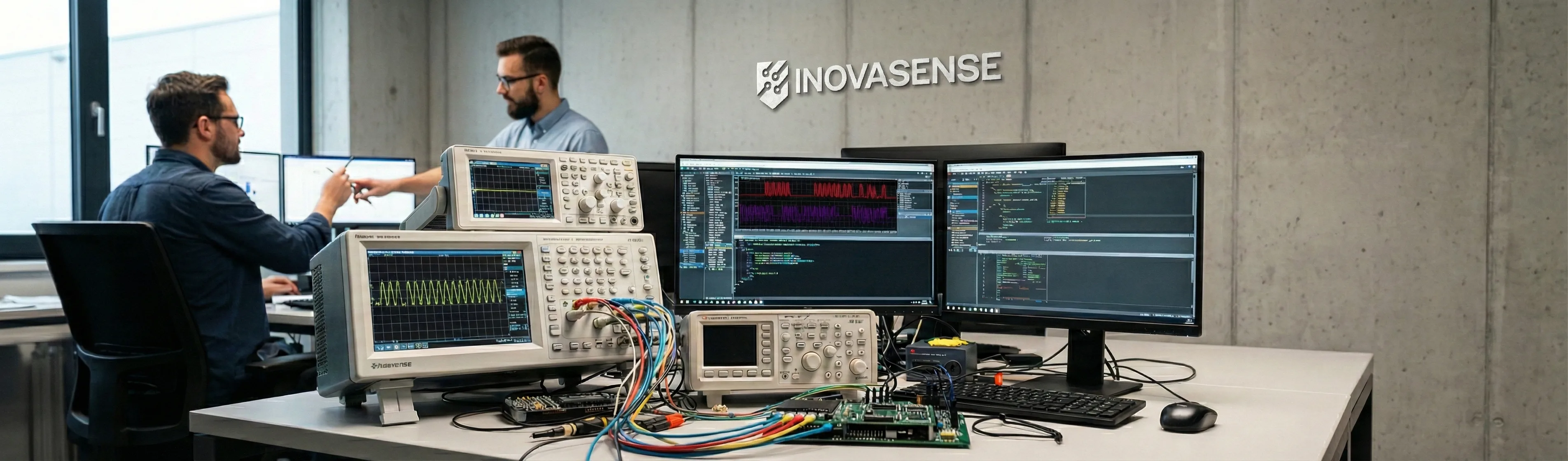
How Inovasense Can Help
At Inovasense, FPGA design is a core competency. We help European companies develop FPGA-based products from concept through production:
- Architecture & feasibility — selecting the right FPGA family for your requirements and budget
- RTL design & verification — VHDL and SystemVerilog, with full simulation and formal verification
- Signal processing — radar, communications, and Edge AI inference pipelines
- High-speed interfaces — PCIe Gen4/5, 10G/25G Ethernet, DDR4/5
- Board design — complete PCB and enclosure design for FPGA-based systems
- EU compliance — CE marking, CRA readiness, and dual-use export classification
- Production support — DFM optimization, component sourcing, quality assurance
Whether you need a complete FPGA product or a single IP block, we bring the full V-Model development methodology to ensure your design is correct, manufacturable, and compliant. Contact us to discuss your project.
Sources & Official References
- Cyber Resilience Act — Regulation (EU) 2024/2847 — EUR-Lex (Official Journal of the EU)
- EU Dual-Use Regulation — Regulation (EU) 2021/821 — EUR-Lex (Official Journal of the EU)